How to Design a Cheap Plant Watering Sensor (Part 5)
published: March 9, 2017 —
last modified: October 23, 2025
This is the fifth part of the meta-tutorial, where I talk about designing a cheap plant watering sensor. If you did not already read the first, second, third and fourth part, please do it now. These parts contain a lot information which lead to this point of the tutorial.
The fourth part ended with step 20, where I did usability tests and stability tests using the preliminary firmware. This article will focus on designing the final board for the project.
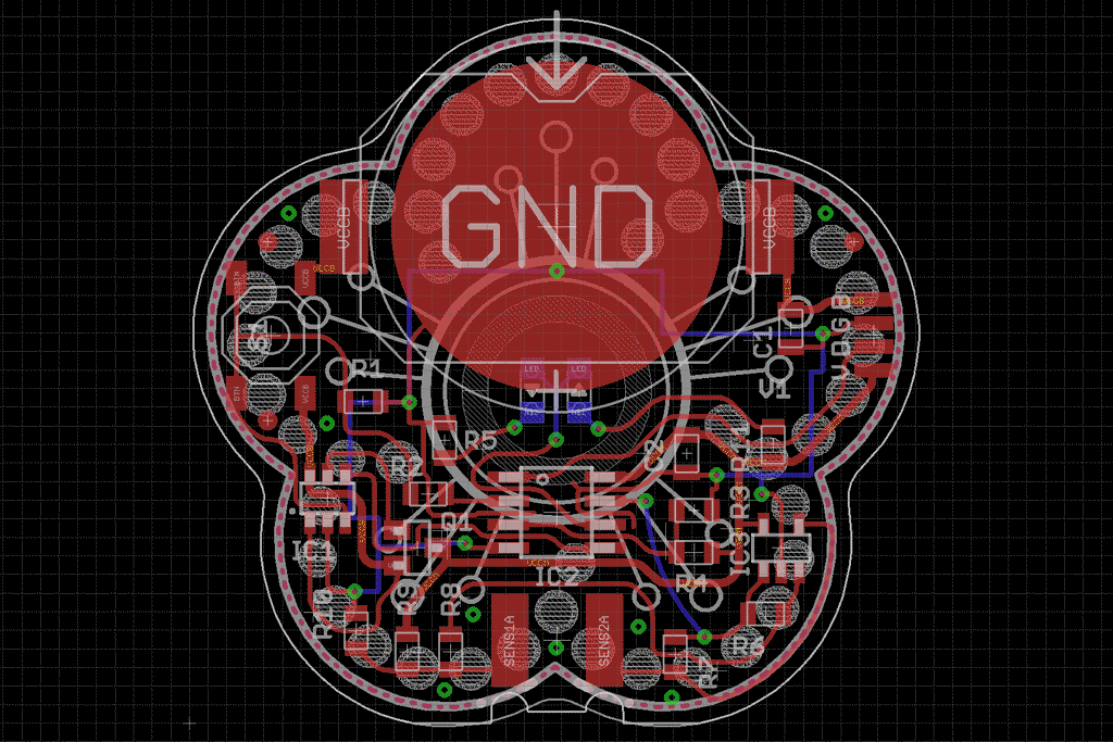
Step 21: Design the Final Board
Designing a good board is like one of these puzzles with quadratic tiles, where you try to lay down a 3✕3 set where all edges match. Often a small change result in many follow up changes, so you have to rip-up a lot of routes and design them in a new way.
My goals for the board were:
Everything, except the two LEDs, should go to the top side of the board.
Reduce the amount of vias to the absolute minimum.
Create a ground pour, especially around the oscillator part, to reduce noise.
Move the button as far as possible from the oscillator to minimise the influence if the user presses the button.
Make it as small as possible.
I worked with small iterations, checking the design after each iteration and checked the design against my goals. To keep track of the changes, I versioned each larger iteration. This way I could go back at a later stage for comparison or if a change did not turn out well.
The Tools
I worked with Autodesk Eagle to create the board. This tool is in the current state far from perfect, but it is cheap and has all required features for the task. For me personally, these are the features I need to design a board:
Smart routing editor which is linked to the schema.
Quick and easy way to create vias and see the required connections.
Good library support for symbols and packages.
Design rule checks.
Quick board preview to check label placement and design.
As you can see, these are not very advanced features and are supported by almost all good board editors. I never use the auto router, because I do not have time pressure or have to do repetitive tasks.
Create the Board Shape
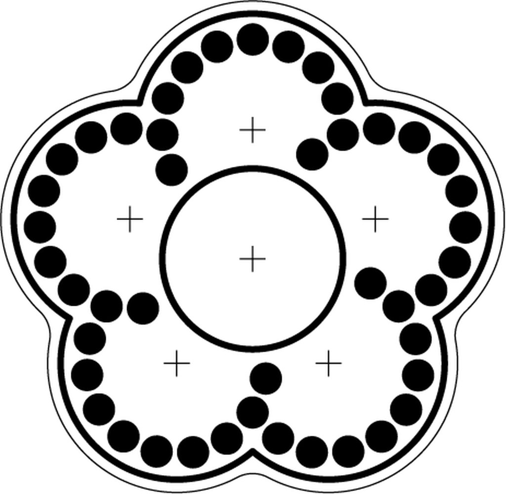
Eagle lacks any tools for design, so I create the initial draft of the board in Adobe Illustrator. Here I convert all curves into straight lines and export everything in DXF format. From there, with a little bit luck, it can be imported into Eagle.
In Eagle, I first move everything to the right place. Next I change the board outline to the Dimension layer and everything else to the Document layer.
Now I had to create all the polygons, because Eagle lacks any usable polygon import. Here I just used a very fine raster and traced the polygons for all copper pours and the solder mask areas where the points should be visible.
The Components
The prototype board was quickly made, so when I started designing the final board, I started from scratch. After importing the outline I placed the components in a way to reduce the route distances. Here I focused on the chips and these elements which have some location restrictions, like the battery holder and the pads for the wire at the bottom.
All small components, like the resistors and capacitors, can be placed in a more flexible way. Therefore I just place them near the place where they are used. When I start to draw routes, I have a better view for good locations of them.
I started with the power routes, because they tend to split the board into sections and are hard to place in a easy way. I also drew routes for all ground connections, these will get obsolete with the ground pour, but I like to be sure there are short connections between all ground pins on the board.
Iterations
In the next sections I will briefly point out the changes I did between the different versions of the board. These iterations are sometimes very small.
Version 2 (Protoype)
This was the prototype board, I just added it for comparison. It has a width of 49mm and is therefore more than 10mm larger than the final board. There was no size pressure and I could place the components freely without any troubles.
Version 3
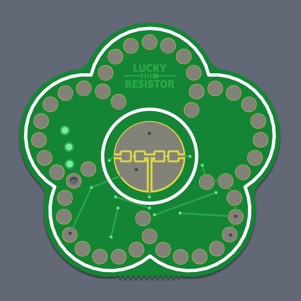
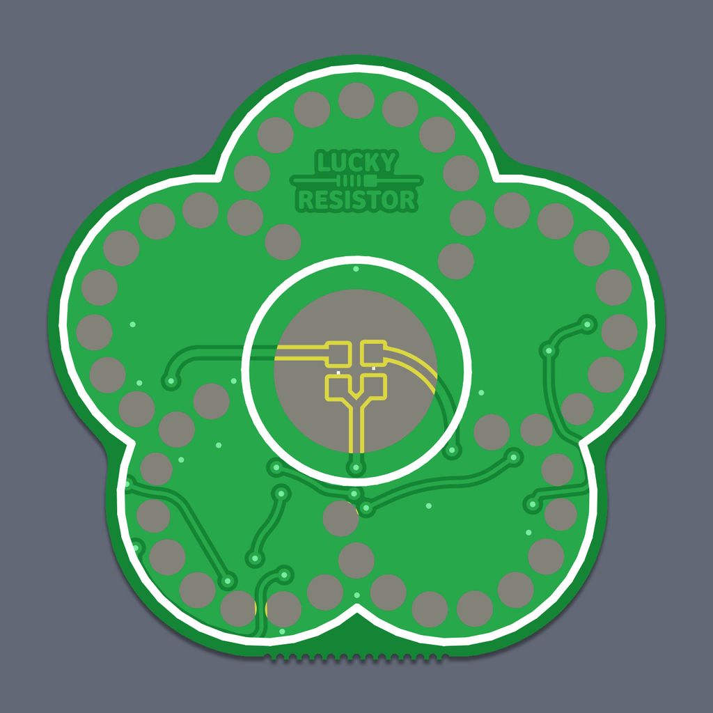
In the first version of the final board, I added the foot of the sensor as a break-apart part below the head. You can see even the traces which connect to this part. It is an idea I dismissed later, because of various problems with the production.
This version still has one LED, because I created the board before the final tests with the prototype to see how small I can go with the board.
Version 4
With this iteration I added the second LED to the design and had to change the routes slightly to do this. I also connected the fourth pin of the debug adapter to the battery power, so I am able to read this voltage in a reliable way.
Version 5
This version was an immediate step to optimise the break-apart section of the foot.
Version 6
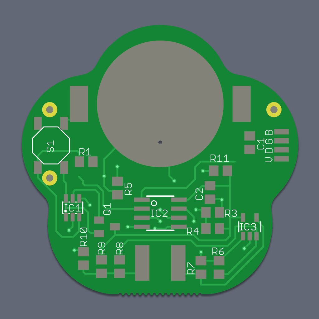
In version 6, I worked on the debug connector. Because it will rarely be used in the final product, I changed it to a small pad based version. It will be connected using an adapter which is normally used to connect to a SOIC chip on the board. It is some kind of clamp I modified, so only one side of the clamp connects to the four pads.
As you can see, changing the debug adapter freed a lot of space, which I use in the next version to optimise the routes.
At this point I also removed resistor R2. Instead of using the perfect value to get a 10 second interval, I use a single resistor which will generate a 9.5s interval.
Version 7
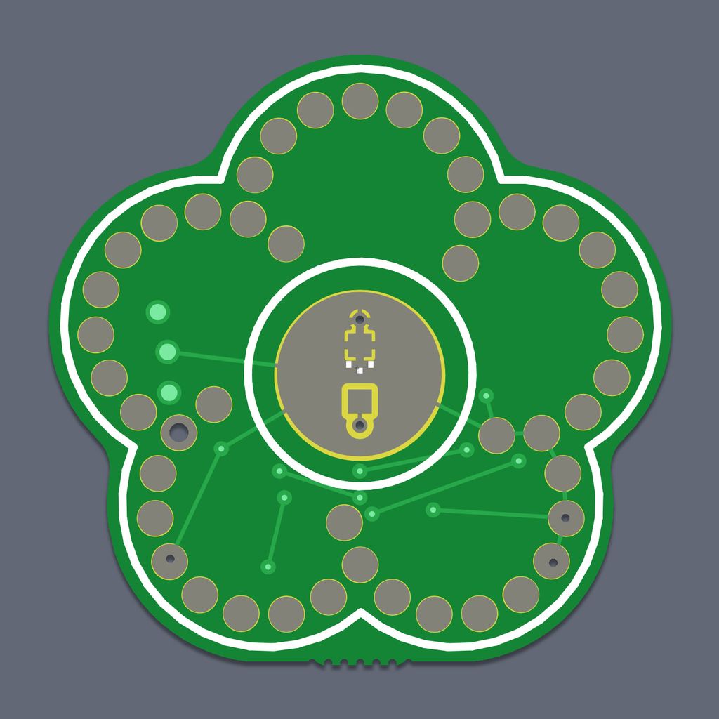
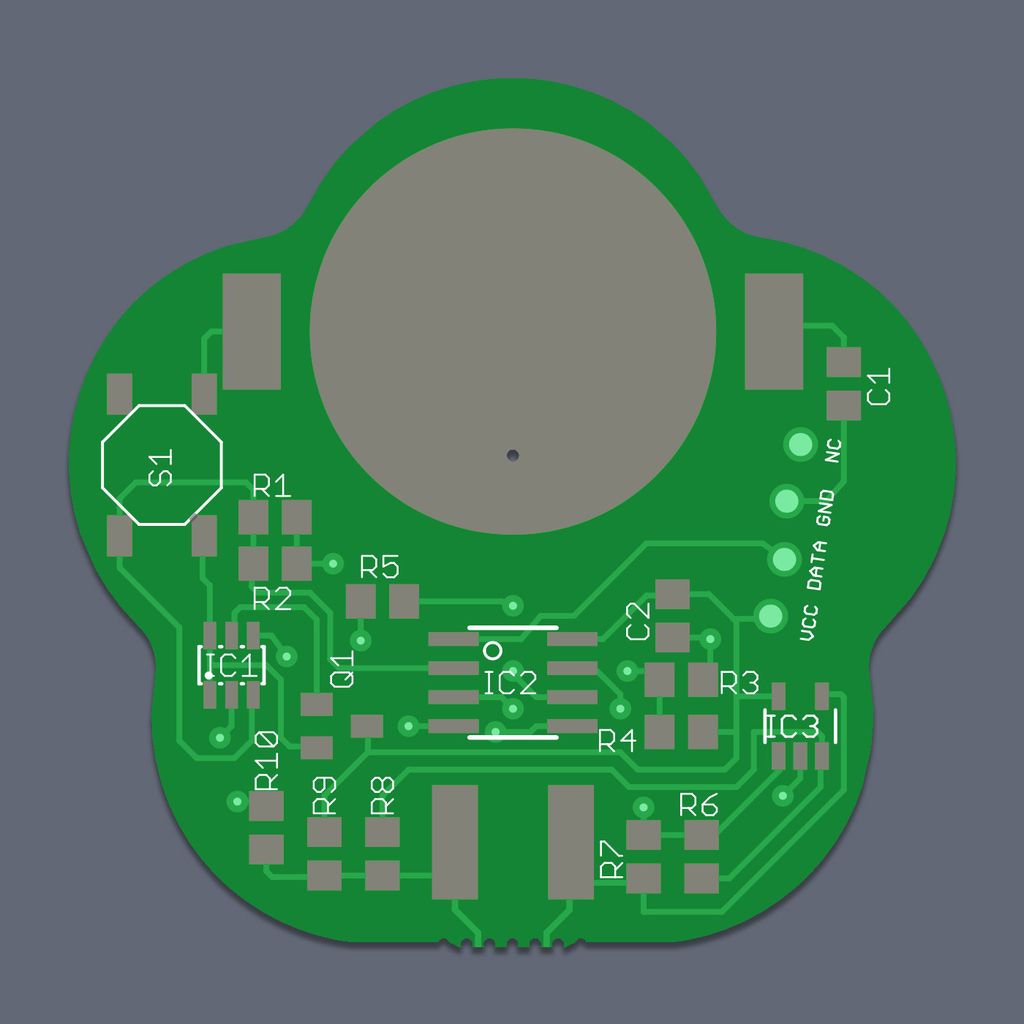
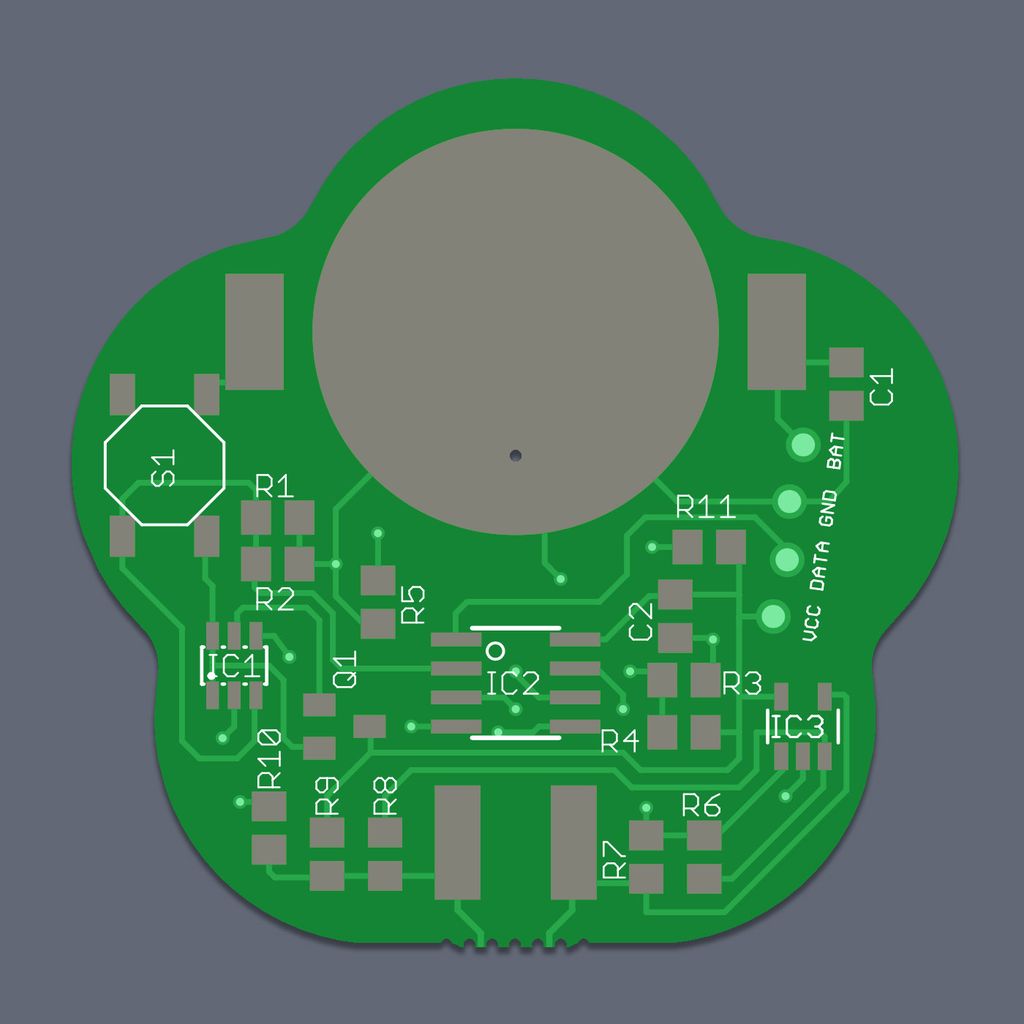
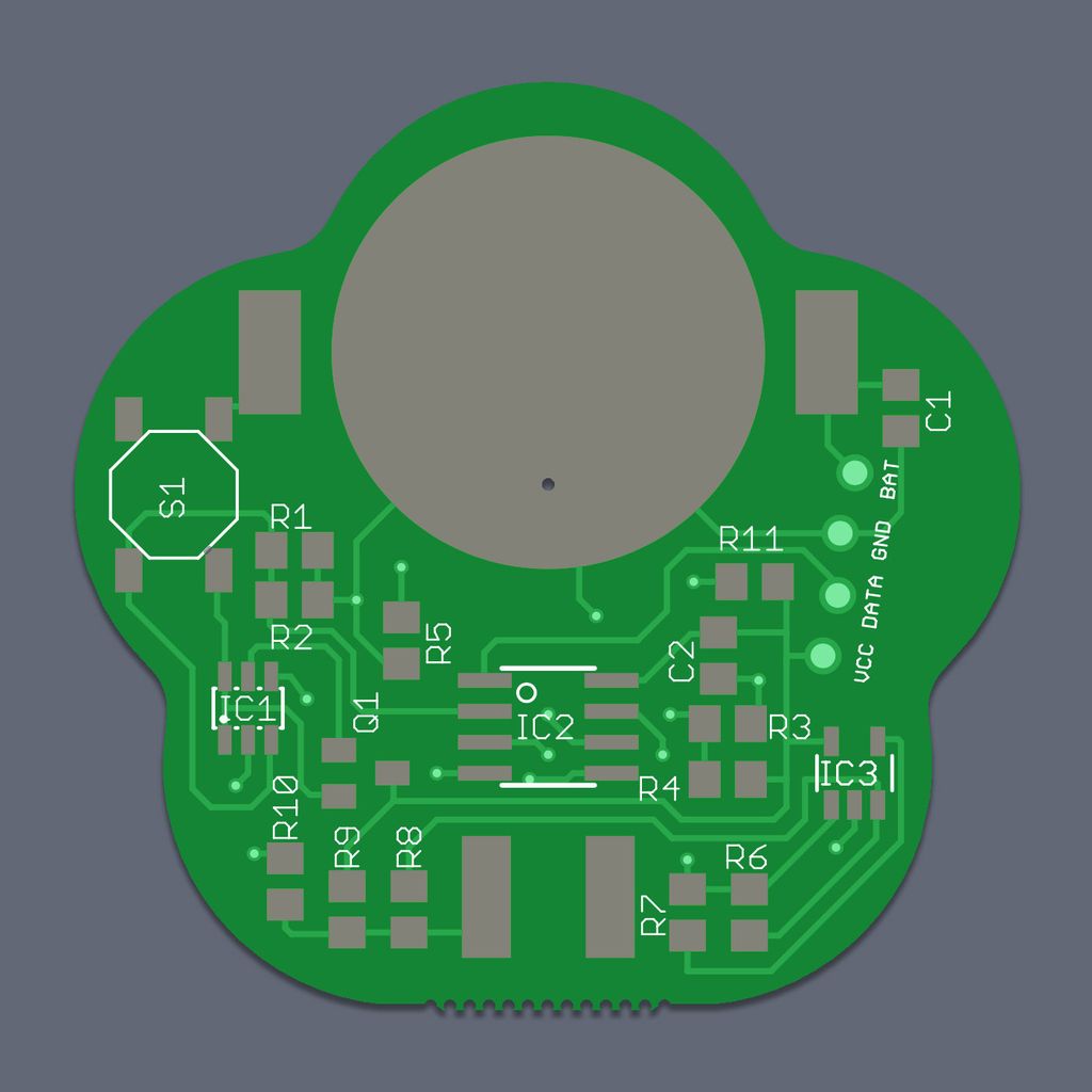
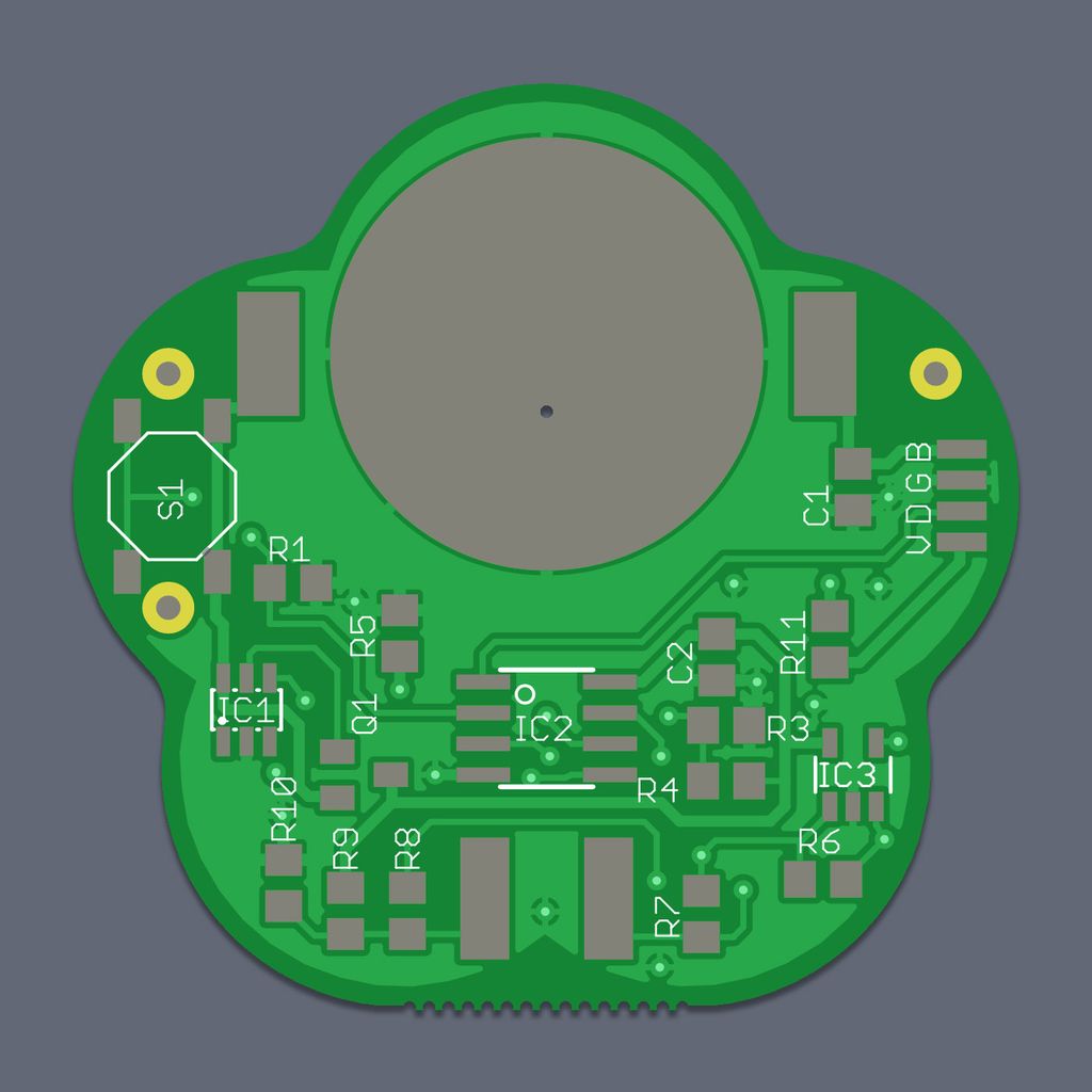
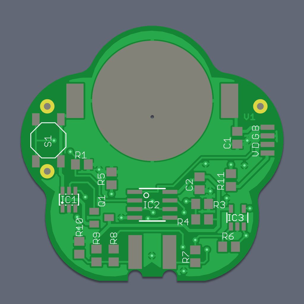
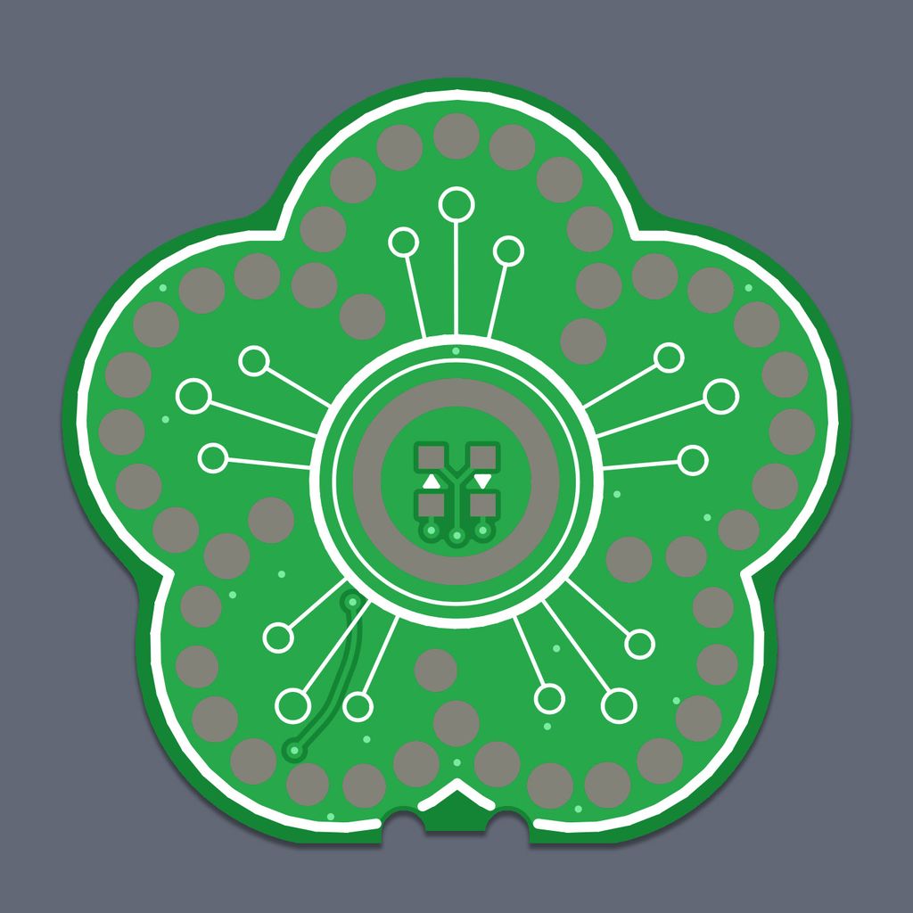
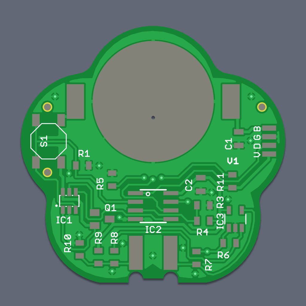
Here I changed the layout of the LEDs to move them to the center. I also worked on the copper pours of the top and bottom side of the board. With the free space from the new debug adapter, I could move the resistors into better positions. Especially resistor R11 was too close to the battery. I like to have some space around the battery to prevent any shorts, even the battery is inserted with too much force.
I added optical alignment points, just to be able to compare the boards easier. Nothing to last for the final version.
Version 8
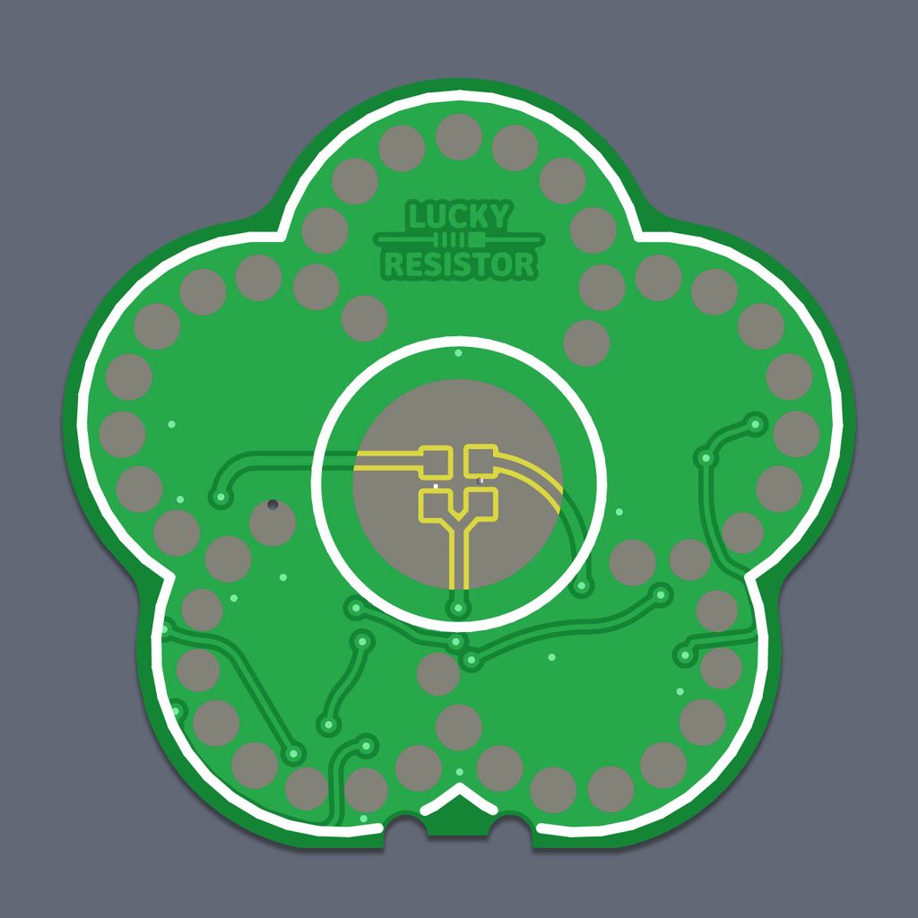
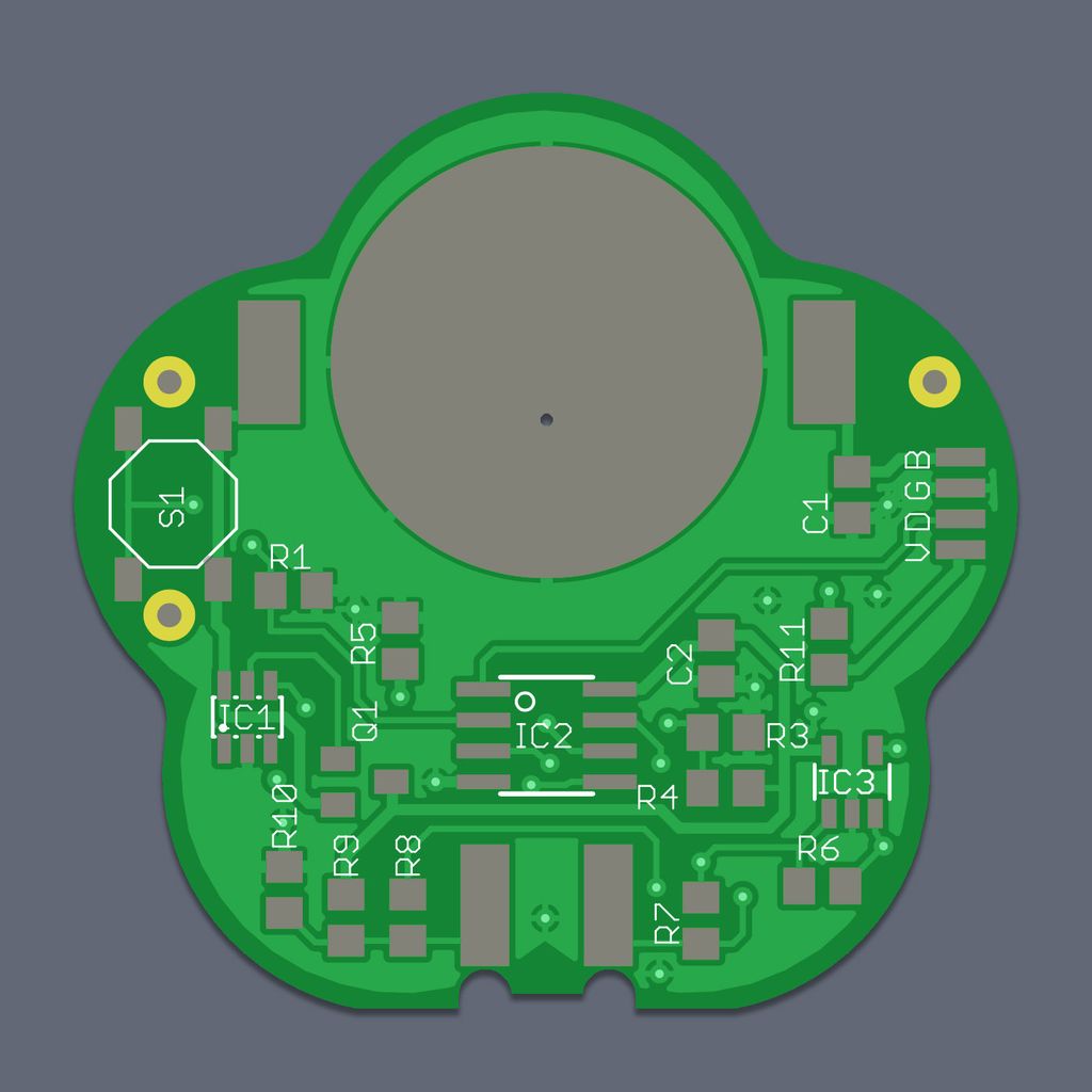
This version was focused on removing the foot part from the board. I added this milling gaps at the bottom to provide room for the insulation of the wires which are soldered to these pads. The wire will lay absolute flat on the pads this way, this makes any bending obsolete after soldering. It also helps to place the wire at the right position.
I ordered a prototype board from this version (without the misplaced via) from Eurocircuits, to get one board for further testing and have some reference for the final size.
Version 9
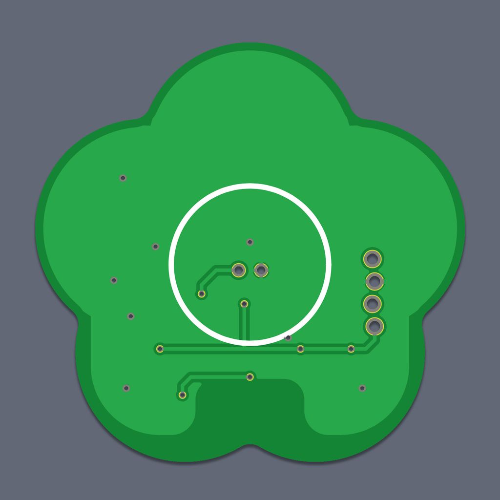
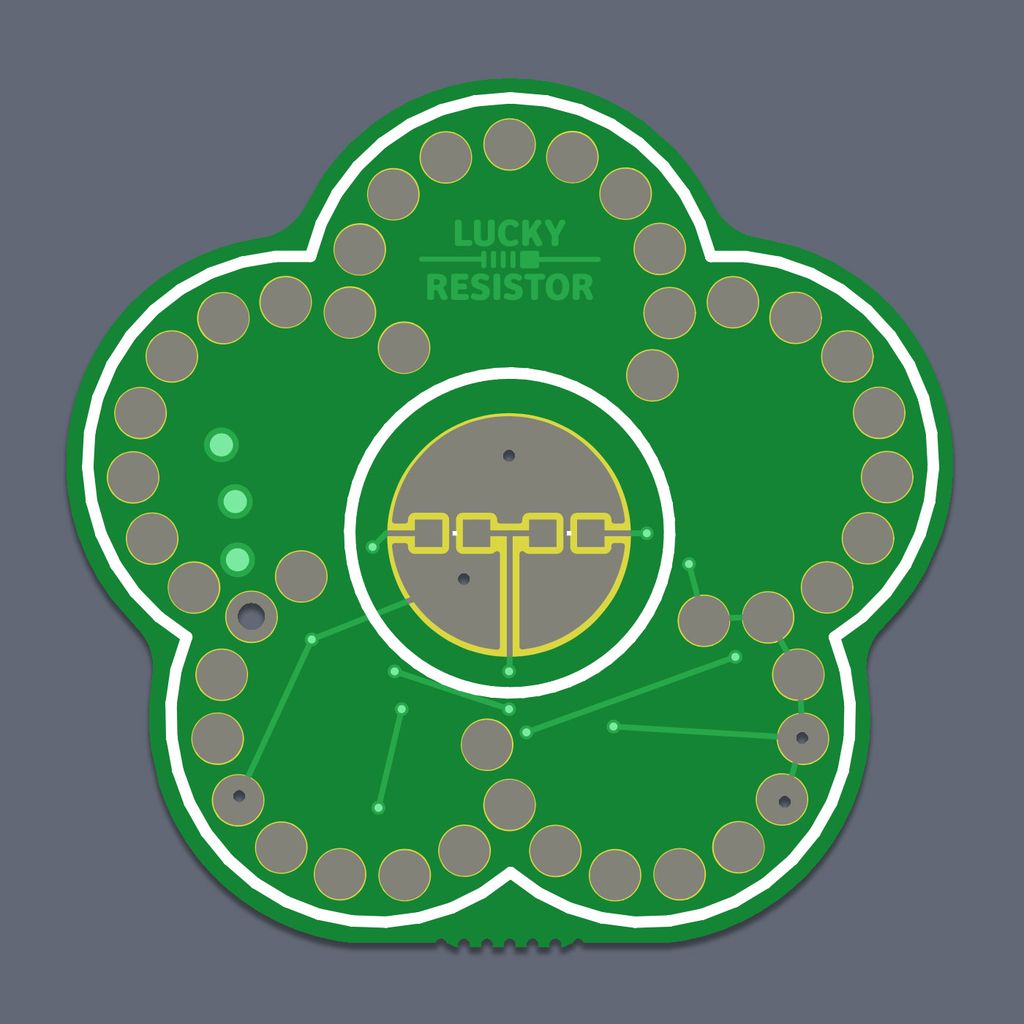
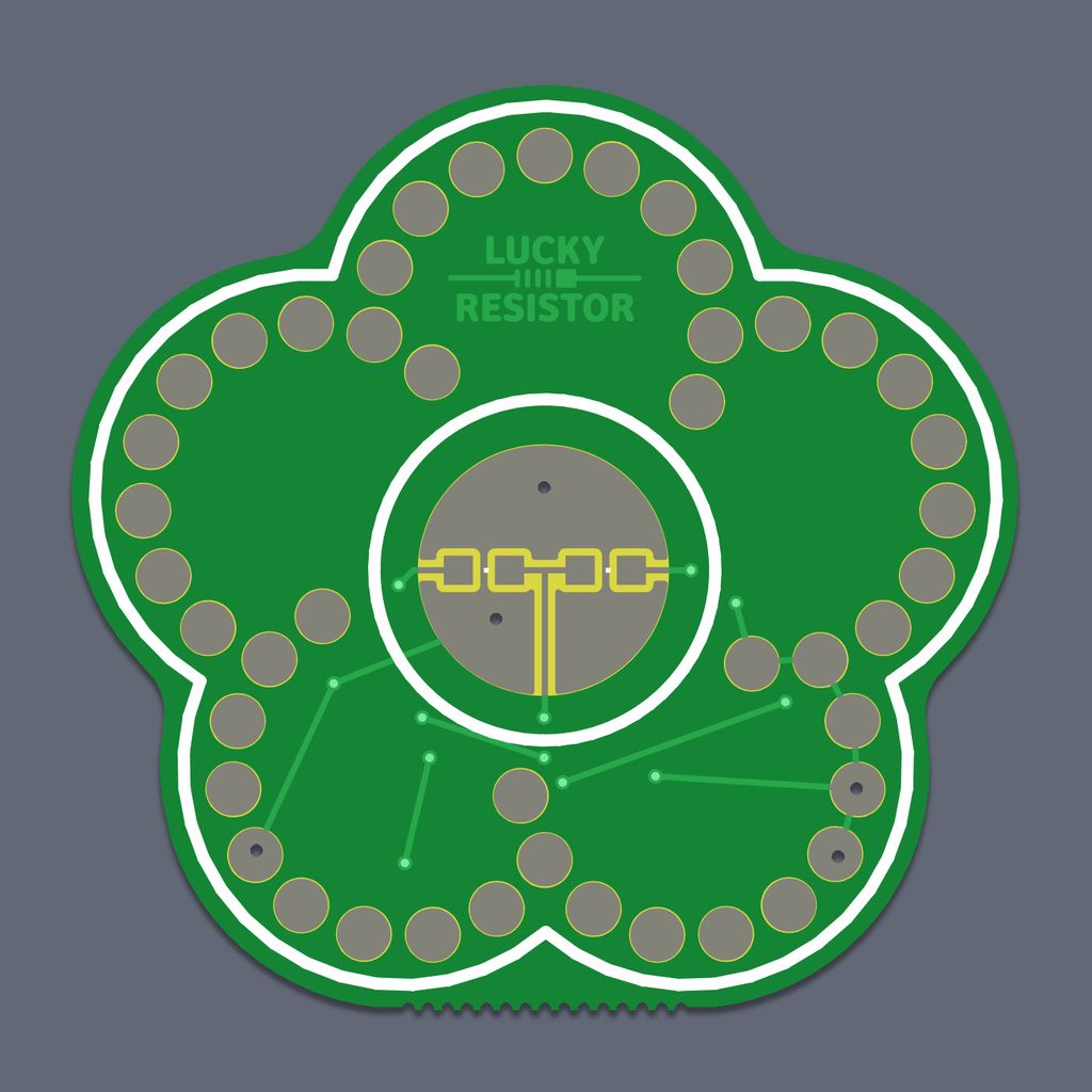
In this version I fixed all problems I found on the ordered board. My original idea, the LED will reflect nicely from the bare copper in the middle was a bad idea. These two LEDs need to be hand soldered, and it is very tricky to do this without a proper solder mask there.
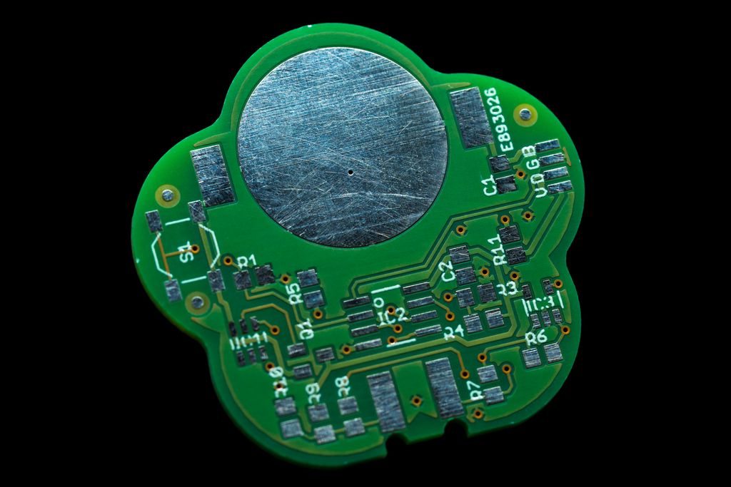
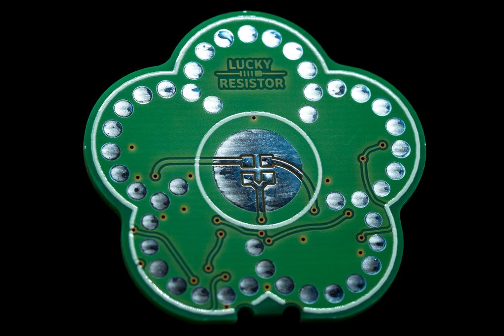
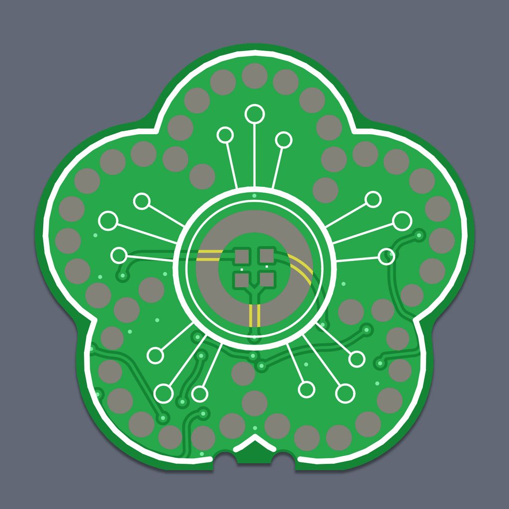
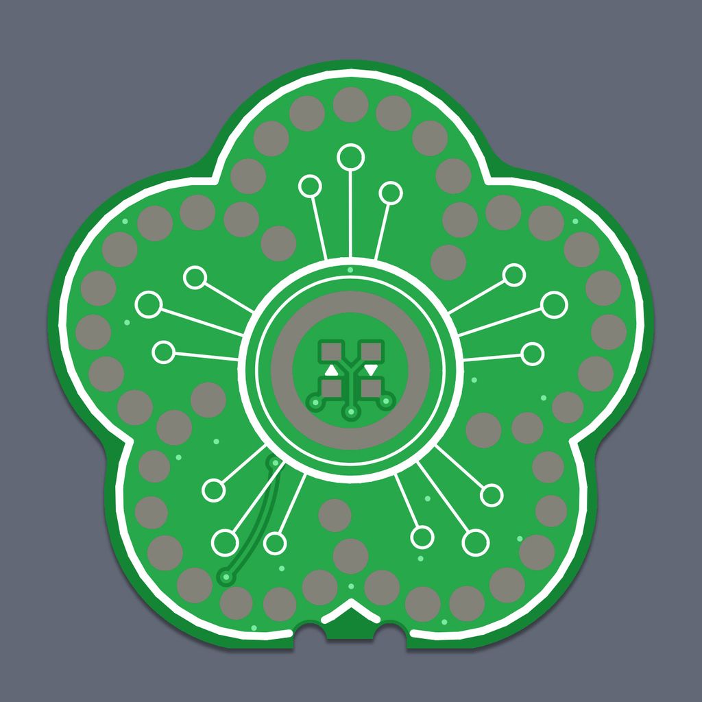
I also added the decoration elements to make the board look more like a flower.
Version 10
In this version, after all components settled into the right positions and testing was successful, I started optimising the routing. I also had the final BOM defined, so I went and updated the package layouts to exactly match the ordered parts.
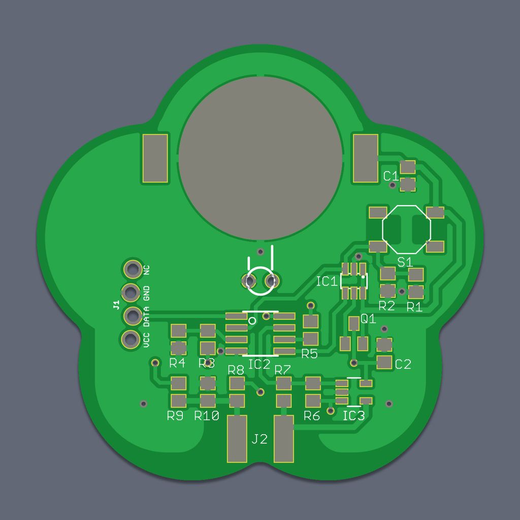
As you can see, I replaced the hand solder resistor pads with ones for reflow soldering. The gap between the pads allowed a more aggressive reduction of vias and routes on the bottom layer.
On the bottom layer I especially removed all routes I could, and added better markings for the LEDs in the middle.
Another focus was the readability of all labels and their placing on the board. The lines of the vector fonts were a little bit small, so I increased all lines to the recommended minimums.
Version 11
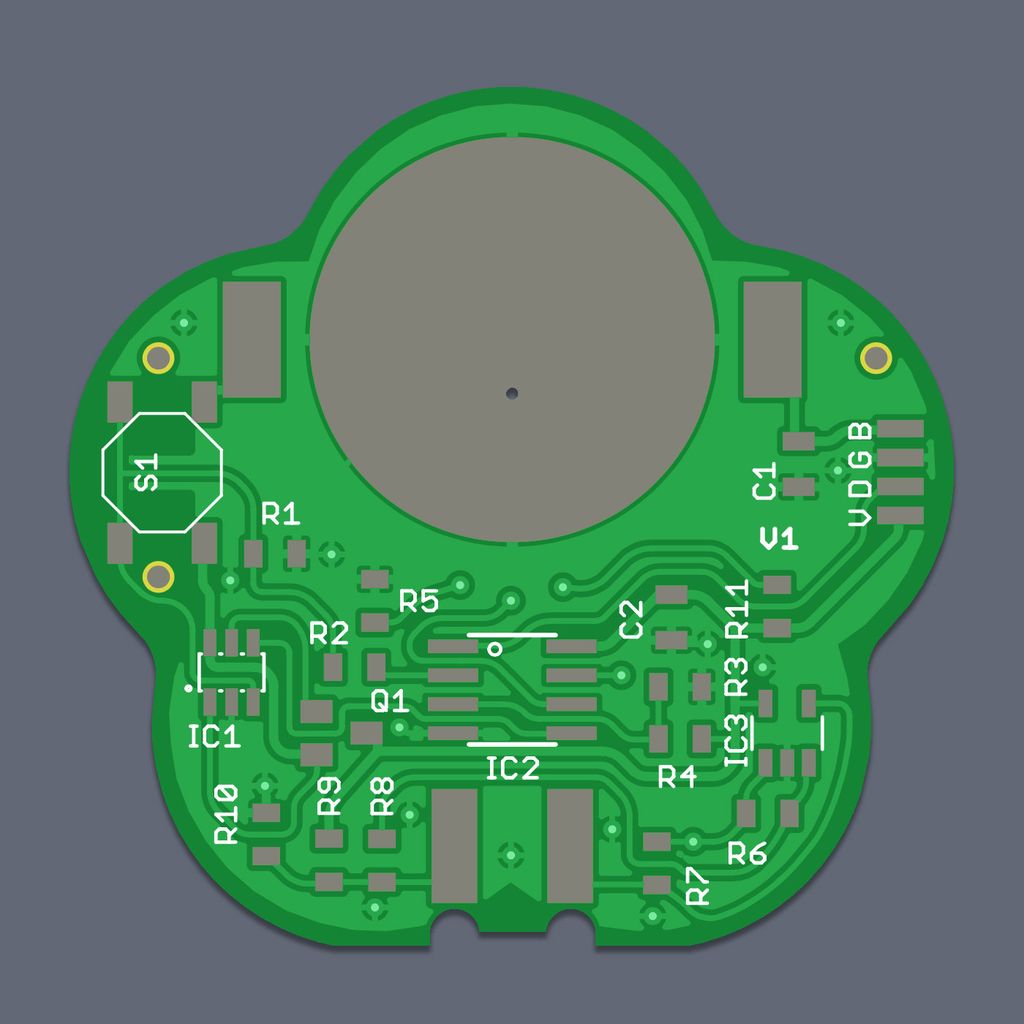
Here I only focused on the copper pours and optimised them to especially enclose all routes which carry any frequency from the oscillator.
This is almost the final design for production. All further changes are barely noticeable. I added more markings to make the locations of the components better visible and shifted the labels slightly. I also removed the optical marks in preparation for the production.
Step 22: Define the Final Bill of Materials
Step 21 and 22 are actually something I did in parallel. You need to fix the final components so you can use the correct pad layout - and without the final design of the board, it makes no sense to fixing the BOM.
I use the BOM tool from Octopart to manage the list of components. It is incredible useful, because you always have the total cost and availability of all your components in plain sight.
Here the list of components for the first batch of devices:
Qty
Manufacturer MPN
Reference
Distributor Unit Price
Total
1
Texas Instruments TPL5110DDCR
IC1
Mouser EUR 0.58
EUR 0.58
1
Microchip ATTINY13A-SSHR
IC2
Mouser EUR 0.46
EUR 0.46
1
Microchip MCP6L01T-E/OT
IC3
Mouser EUR 0.18
EUR 0.18
1
Fairchild Semiconductor BSS84
Q1
Mouser EUR 0.06
EUR 0.06
1
KOA Speer RK73H2ATTD1102F
R1
Mouser EUR 0.007
EUR 0.007
2
KOA Speer RK73H2ATTD1502F
R2;R4
Mouser EUR 0.007
EUR 0.015
2
KOA Speer RK73H2ATTD82R0F
R5;R11
Mouser EUR 0.007
EUR 0.015
6
KOA Speer RK73H2ATTD4702F
R10;R3;R6; R7;R8;R9
Mouser EUR 0.007
EUR 0.040
2
Murata GRM21BR71C105KA01L
C1;C2
Mouser EUR 0.025
EUR 0.051
1
SloanLED SMD-G0805-02
LED1
Distrelec EUR 0.16
EUR 0.16
1
SloanLED SMD-R0805-02
LED2
Distrelec EUR 0.05
EUR 0.05
1
Linx BAT-HLD-001
BT1
Mouser EUR 0.22
EUR 0.22
1
ALPS SKQGAKE010
S1
Mouser EUR 0.11
EUR 0.11
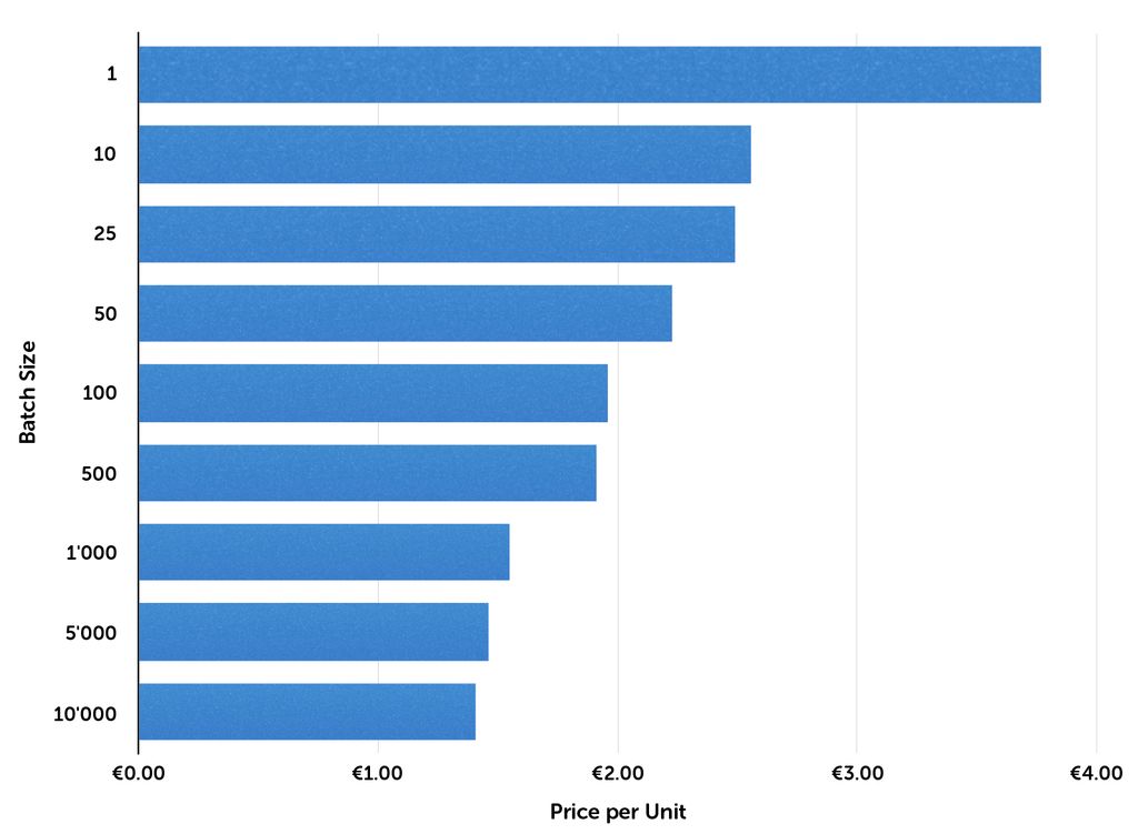
Starting from a batch size of 100, the price difference gets minimal until you reach 1000 and more. The next diagram shows the unit price, related to the batch size:
Step 23: Plan the Assembly
To assemble a small batch of devices in a fast an efficient way, the best would be to let a manufacturer produce the boards and assemble them. This would be nice and easy, but would take the fun, of assembling the boards by hand, out of the project. :-)
The fastest way to assemble the device by myself is using panels with a stencil and hot air. So I can prepare one or more panels with solder paste, add all components to them and flow soldering most of the components. There is a little bit work left to solder the battery holder, the two LEDs and the wires in place, but this is fast and easy work - compared to all the small resistors and chips.
I found out, the most economic panel size for the project is a grid of 4×2 boards for the head part. For the foot parts with the sensor plates, best is to let the manufacturer produce them as single boards and panel them as he likes.
Each sensor plate (foot) also requires a heat shrink tube, to protect it from the microorganism in the soil and protect them from the copper in the board. Copper is toxic for microorganisms, so it should never come into contact with the soil.
Step 24: Calculate the Total Cost
“Hidden” Costs
The table does not contain costs for additional material like the two pieces (=40cm) of wire for each sensor (~EUR 0.1) and for the solder paste for each board. The solder paste is: ~56mm² × 130µm = 7.28mm³ per unit. This is just a very rough estimation, there is always some waste and paste stuck in the stencil.
With a cost of EUR 0.0013 per mm³ for the solder paste, there is additional ~EUR 0.01 per unit for the solder. Also a small amount of solder is used for the LEDs and to solder the wire to the device, here I found this is just additional ~EUR 0.001, nothing to worry about.
Each sensor foot needs 40mm hot shrink tube to protect the PCB from microorganism in the soil. This is additional EUR 0.07 per unit.
I do not calculate any cost for the labour used to assemble and develop this project, because this is no commercial enterprise and I do this for fun. But this would be part of any professional calculation.
There are also other costs which are not included here, but can get important for a real calculation:
Shipping fees for component and board orders.
Energy costs (Soldering, Hot Air, Heating, Light)
Storage, working place costs (Rent)
Amortisation of tools (Things will break, you need to buy new or newer ones)
Software license costs
Manual (Print costs, translations)
Packaging (Print costs, packaging costs)
Packaging for shipping.
Costs for sales system (Webhosting, etc.)
Taxes
As mentioned in the sections above and below, just to make the list complete:
Labour cost for preparation, assembly and packing.
Labour cost for development.
Board Prices
For the board, I have two components: The “head” and the “foot”. I found out, the cheapest way to produce them is to panelize the head into a 4×2 grid and produce the foot as single boards by the manufacturer.
With these parameters I get EUR 1.51 per unit for the head part and EUR 1.16 per unit for the foot part. All boards are produced at a very high quality, with blue solder mask from Eurocircuits.
Development Costs
It is important to add the development cost to the calculation. This is not a factor for the calculation of the unit cost for production, but an important value to calculate a price for sale. The price to sell one unit should always be based on the production unit cost + development cost divided by the first batch of sold products. Calculating the price this way, you ensure you get the development costs back by selling the first batch of products. Obviously the final price contains other factors as well.
In my case, there are prototype boards and initial test component orders. Also I created a programming adapter to pre-program the microcontroller. All this will sum up, including various shipping fees.
Unit Cost Summary
With all this collected costs, we get the following summary. Best is if you create some dynamic spreadsheet, where all this costs automatically are calculated based on batch sizes. The following table is calculated for a batch size of 100-200 units.
Item
Cost per Unit
Components
€1.96
Boards
€2.67
Wires
€0.10
Solder Paste
€0.01
Hot Shrink Tube
€0.07
Assembly Labour
€0.00
Development Material
€2.00
Development Labour
€0.00
Epilogue
Thank you for reading this article! I hope it was insightful as the last parts and will help you with your own projects.
I'll walk you step-by-step through printing the mechanical parts of a fully functional, programmable cat/pet feeder. I share STL files, material and printer recommendations, and parts lists — all open-source on GitHub. If you have a 3D printer and want a challenging build, read the full post to get started.
I guide you through writing a near-final firmware for my cheap plant watering sensor, describing module structure, incremental development, and practical tests. I cover ADC sampling, oscillator checks, EEPROM settings and a prototype fix for the push-button. If you’re building a similar device, I invite you to read the full post.
I walk through the sensor board I designed for the pet feeder, explaining the position sensor, four fill sensors, and why component choices (like the 100kΩ resistor) matter. I keep the design simple and practical — read the full post for schematics, measurements, and ordering details.
I tried mixing epoxy in a plastic cup and caused a small meltdown — a useful reminder about heat, cure times, and containment. I share what went wrong, safety and cleanup tips, and practical fixes to help you avoid the same mistakes. Read the full post for step-by-step guidance.
Posted on 2019-07-23— C++, Improve your Code, Learn
I explore replacing unsafe bit macros with lightweight C++ templates to make embedded bit operations safer and clearer. I show templates for one-bit extraction, set/clear helpers, and compiled firmware size for Arduino Uno. Read the full post to see examples, exercises, and practical benefits.
I use Autodesk EAGLE regularly and, while I appreciate parts of it, I ran into 12 recurring issues that waste time and hinder workflow. In this article I explain each problem and suggest improvements. If you use EAGLE, please read on — I hope it helps.